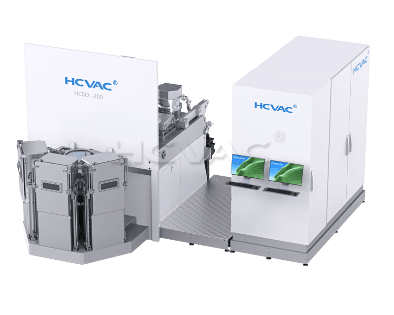
ICP-assisted magnetron sputtering enables optical coatings with low absorption and low film stress. It is used to fabricate bandpass and cut-off filters, such as Face ID optics and high-transmittance mid- and long-wave infrared coatings.
The system supports magnetron sputtering of metals including Cu, Al, Cr, Au, Ag, and SUS. Process development improves coating performance in deep features. The deposited films provide excellent step coverage and are used in MEMS chip packaging.
Key Features
Compatible with automated substrate handling systems for 4–12 inch wafers
Real-time, direct on-substrate monitoring during deposition
Clean deposition environment with few point defects
Stable deposition processes with high repeatability
Fast target change and easy maintenance
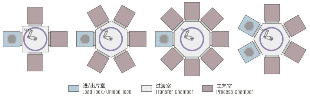
Flexible Modular Cluster System
The equipment adopts a modular design. It can be integrated with plasma cleaning units, magnetron sputtering (SPT) units, plasma-enhanced chemical vapor deposition (PECVD) units, atomic layer deposition (ALD) units, and reactive ion etching (RIE) units.
These modules can be combined into a cluster processing center. The system covers substrate cleaning, thin film deposition (including ultra-thin films), and patterned etching for semiconductor micro- and nano-structure fabrication.
The system meets strict film deposition uniformity requirements. It minimizes high-stress film-related defects. This helps increase yield and reduce manufacturing cost.
Modular design for easy upgrade or retrofit. Provides customers with ideal system configurations.
Independent process chambers. Enables flexible switching between different processes.
SPT: Deposits a wide range of materials. Co-sputtering mode is available.
PECVD: Used for various optical coating materials. Refractive index (n) and extinction coefficient (k) are adjustable.
ALD: Deposits ultra-thin films. Provides uniform films with high conformality.
RIE: Etches multi-layer films of different materials. Enables precise control of sidewall verticality and trench profile.
Application Cases
High-precision optical components
MF / RF reactive sputtering of oxide and nitride films
Wafer packaging
DC / DC pulsed sputtering of metal films
Barrier layers of semiconductor devices
Deposition of ultra-thin films by ALD
Biomedical
Metalization of medical devices, controlled-release layers for pharmaceuticals
Microcircuits
RIE for patterned film etching using photoresist masks
Hello Can we help you? We have over 20 years of experience in the PVD field. If you have any requirements, please feel free to contact us via WhatsApp.