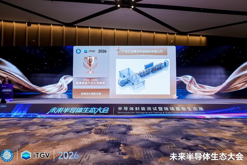
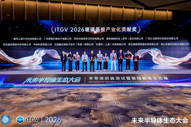
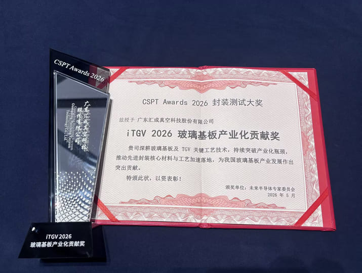
On May 29, at the 2026 Future Semiconductor Ecosystem Conference and CSPT Awards 2026 Ceremony held in Wuxi, HCVAC received the "iTGV Glass Substrate Industrialization Contribution Award" for its independently developed Deep Via Glass Sputtering System.
The award was jointly selected by an expert panel consisting of nearly 40 universities, research institutes, and industry organizations, including Tsinghua University, Shanghai Jiao Tong University, Jiangcheng Laboratory, JCET, and Tongfu Microelectronics.
It recognizes companies that have made outstanding contributions to glass substrate materials, TGV process development, key equipment validation, and industrial applications.
The AI Era Is Accelerating the Industrialization of Glass Substrates
With the rapid development of AI foundation models, High-Performance Computing (HPC), High Bandwidth Memory (HBM), Chiplet-based heterogeneous integration, and Co-Packaged Optics (CPO), advanced packaging has become one of the most important areas of innovation in the post-Moore era.
As a key platform for next-generation advanced packaging, Glass Core Substrates offer several advantages, including low warpage, excellent dimensional stability, superior high-frequency performance, and ultra-high interconnection density. As a result, they are becoming a major focus of investment across the global semiconductor industry.
Today, leading companies such as Intel, Samsung Electro-Mechanics, LG Innotek, TSMC, ASE, and Absolics have all launched glass substrate research and industrialization programs. Glass substrates are widely regarded as an important foundation for future AI servers, HBM4/5 memory, high-speed switching chips, and silicon photonics interconnects (Source: TrendForce).
In China, companies such as WG Tech (Vog Optoelectronics) and Chengdu ECHINT Technology Co., Ltd. are actively advancing glass substrate manufacturing and TGV process development. At the same time, advanced packaging companies such as JCET and Tongfu Microelectronics continue to explore the application of glass substrates in next-generation packaging architectures, helping to accelerate the development of the industry ecosystem.
Advanced Packaging & TGV PVD Platform
Next-Generation Metallization Technology for TGV and Heterogeneous Integration
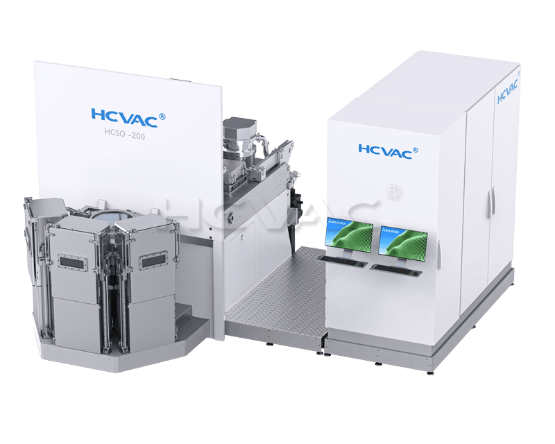
HCVAC's Advanced Packaging & TGV PVD Platform is designed to support Through-Glass Via (TGV) processing and heterogeneous integration, providing next-generation metallization solutions for AI and semiconductor substrate applications.
High Aspect Ratio Metallization
The platform achieves excellent seed layer coverage inside deep TGV structures, supporting aspect ratios of up to 15:1.
Cluster-Type Coating Platform
The fully automated cluster platform integrates pre-cleaning, sputtering deposition, and degassing modules. It is compatible with both 6-inch to 8-inch wafers and glass panels, enabling efficient and stable production.
Excellent Adhesion Performance
The system is optimized to ensure reliable adhesion between Ti/Cu seed layers and glass or polymer substrates, making it suitable for Redistribution Layer (RDL) fabrication.
TGV Metallization: A Key Process for Glass Substrate Industrialization
In glass substrate production, Through-Glass Via (TGV) metallization is the core process for achieving high-density vertical interconnections.
For glass vias with diameters as small as 20 μm and aspect ratios greater than 15:1, achieving continuous, uniform, and reliable seed layer deposition along the via sidewalls remains one of the key technical challenges for large-scale manufacturing.
To address this challenge, HCVAC has developed a dedicated Advanced Packaging & TGV PVD Platform. Powered by its proprietary deep via glass sputtering technology, the system enables seed layer deposition in high-aspect-ratio TGV structures, providing a critical foundation for subsequent copper via filling and RDL processes.
Main Technical Specifications
Deep Via Sputtering
- Minimum via diameter: 20 μm
- Maximum aspect ratio: 15:1
- Compatible with substrate sizes up to 700 × 700 mm, as well as 310 mm, 510 mm, and 600 mm formats.
- Step coverage: above 6%
RDL Applications
- Surface uniformity: ≤ 5%
- Dense and smooth copper film
- Adhesion strength: ≥ 8 N/cm³
- Compatible with substrate sizes up to 700 × 700 mm, as well as 310 mm, 510 mm, and 600 mm formats.
The technology has already been validated for a wide range of applications, including advanced packaging, glass substrates, Chiplets, HBM, silicon photonics chips, and Co-Packaged Optics (CPO).
From Equipment Innovation to Industry Collaboration
This award not only recognizes HCVAC's technological innovation in TGV metallization equipment, but also highlights the growing role of Chinese vacuum equipment manufacturers in the global glass substrate supply chain.
Looking ahead, HCVAC will continue to increase investment in advanced PVD equipment development for strategic fields such as advanced packaging, glass substrates, silicon photonics, optoelectronic integration, and AI infrastructure.
Together with industry partners, HCVAC will continue to promote the large-scale adoption of Glass Substrate, TGV, and advanced packaging technologies, helping drive the high-quality development of China's semiconductor industry.